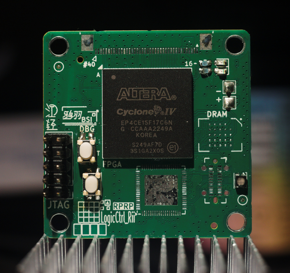
FPGA Development board with Altera's Cyclone IV (LogiCtrl_Rii)

Long and Redundant Introduction
It is a bit hard to explain why I ended up making a FPGA development board.
While I was working with the custom-made X ray inspection device, I ran into issues with the developing solution oxidizing too fast. Also, using dental X ray film does produce decent images of the PCB, especially even the golden bond-wires inside a BGA package can be seen, but it is still single use. Digital sensors are too expensive however, therefore I wanted to build a camera that has long exposure abilities, to image a scintillation screen. After this series of “development”, I ended up with a need for some sort of high speed data receiver.
Last year I have tried working with small, parallel CMOS image sensors with an STM32H7, which some bonded out the “DCIM” interface, which is basically a parallel data Rx interface with some simple processing features. This time however, I was expecting a fancier sensor, something that uses LVDS or MIPI. Typically, this is done by an microprocessor, such as the very famous Raspberry Pi. For my case however, the experience with microprocessors (see the STM32MP157 project) was not very fun. Therefore, I decided to make a FPGA development board to act as a stage between the computer, and some sort of LVDS interface.
Now it comes to decide what FPGA do I want to design for.

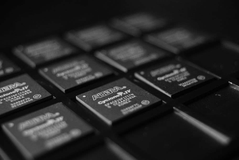
FPGAs are high-end semiconductors. They can be as expensive as modern desktop CPUs (or even more), and the lowest end FPGAs that major companies offer are reasonably expensive. That is true, but a work-around exists - that is the good old Cyclone IV by Altera. Especially, parts like the EP4CE15F17, which is in a 1mm pitch BGA package, can be done with ease with JLC’s 4 layers PCB. They can be also purchased at very low cost from Taobao (the original Aliexpress in China), which is ideal for DIY needs.
Hardware Design
There’s not much “peripherals” to a FPGA, everything is custom designed logic, written in Verilog or VHDL. The only considerations is the capability of the IO pins, some offers differential signalling, some offers a dedicated clock input. Another difference is that usually FPGAs have no internal power regulators; For the cyclone iv, it needs a 1.2V for V~core~, 2.5V for V~analog~, and 3.3V for other supplies. For BOM simplicity, I just used 3 LDOs for each rail, as this is a rather small FPGA chip.
For the on-board memory, the Cyclone IV natively supports DDR2 SDRAM, which is far obsolete even by embedded standards. Therefore, I have routed a HyperRAM on this board, it might seem odd but it’s basically a DRAM wrapped with a built in controller. Interfacing the HyperRAM is similar to a EEPROM; it has 8 data pins (which is a 1 byte bus), 1 clock, 1 chip select, and 1 Read-Write Data Strobe pin. To write, the FPGA writes the address of memory, and shifts in the data byte by byte. As its still a DRAM, there is a maximum length of write operation (given in microseconds since its not clock dependent, bu only time taken for the charges in DRAM cells to fade away). Whenever this upper time limit is reached, the Chip Select (CS) must be asserted high, in order for the internal controller to refresh the chip. (?) Sounds promising… *Since I have not ordered the HyperRAM, it is not tested yet.
The Fatal Bug!!!

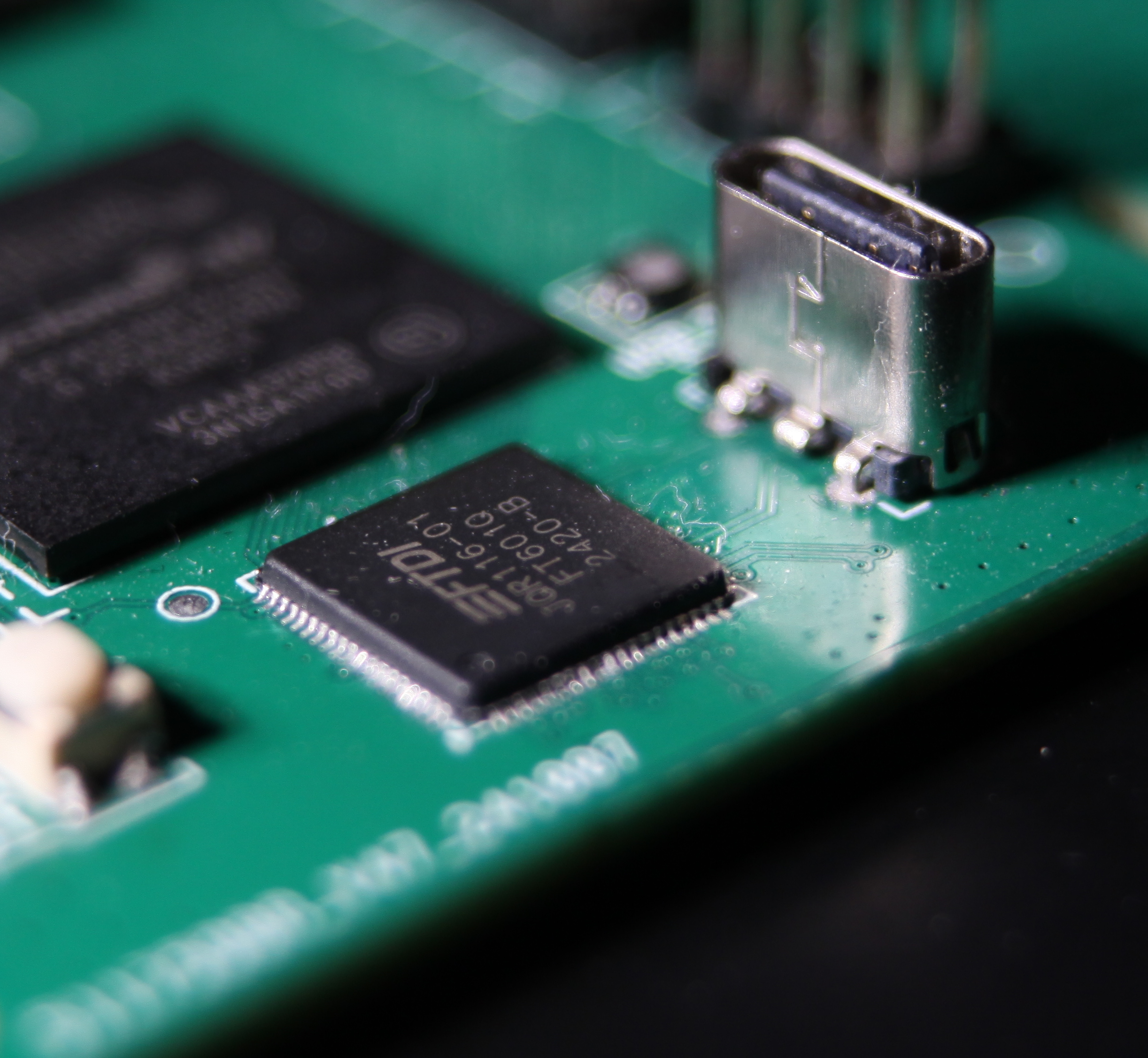
I made a fatal mistake in the pin planning. In the USB3 FIFO chip FT601, some pins of the 32 bit data bus is connected to a clock pin on the cyclone iv. While it might fine, on this FPGA the clock pins can be used as clock input only, so that only 1 byte in the bus is fully connected correctly.
*Anything else on this board should work